 HammBurg Be informed with latest news, reviews, entertainment, lifestyle tips, and much more.

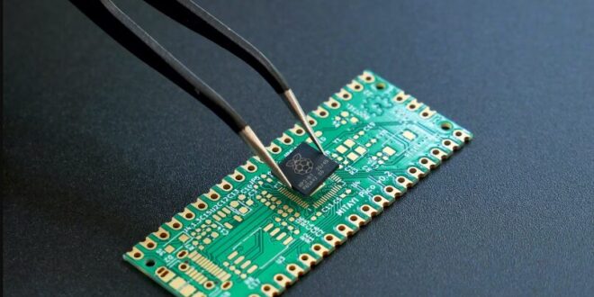
Semiconductors act as the backbone of modern society in terms of enabling advances in transportation, communications, computing, clean energy, etc. Their electrical conductivity is valuable in manufacturing a horde of digital consumer products like televisions, smartphones, LED light bulbs, and washing machines, among others.
But what about the manufacturing process of a semiconductor? Being highly sensitive materials, semiconductor chips are vulnerable to easy contamination. This could lead to issues with production and product failure.
If your facility is involved in manufacturing these chips for computerized devices, you need an exclusive semiconductor manufacturing cleanroom. In this article, we will discuss the four crucial steps involved in the design process.
Semiconductor Cleanroom Classifications
Semiconductors are such that even the slightest contaminant can corrupt them. This is why they must be designed as per the ISO 5 cleanroom classification. This is the same standard that the Federal government follows for manufacturing its research and development facilities.
According to American Cleanroom Systems, cleanrooms designed based on this classification must have 300 to 480 air changes for every hour of HEPA-filtered air. This level of filtration lies on the higher end of the spectrum, with the ultra-low penetration air (ULPA) being 99.9995%.
If your cleanroom is not designed as per these specifications, there will be manufacturing defects leading to product failure.
Threats Involved in Semiconductor Manufacturing
While working in a semiconductor manufacturing cleanroom, operators come across numerous challenges associated with contamination control. The issue sometimes is the human operators themselves.
This happens through particulate matter produced by their bodies and clothing. Other than that, the human body may also generate electro-static discharge (ESD), which threatens to ruin the semiconductor’s electronic circuits.
Besides human contaminants, environmental threats may disrupt the manufacturing process, including humidity, airborne particles, pressure malfunctions, power glitches, and equipment outgassing. This may sound like a lot but semiconductors are so sensitive that even the tiniest speck of dust can damage them.
4 Steps Involved in Designing a Semiconductor Manufacturing Cleanroom
Despite the threats and challenges involved, a well-designed and controlled cleanroom will do most of the heavy lifting on your behalf. When designed correctly, it will offer the level of environmental control needed to optimize productivity.
Let’s look at the four important steps involved in designing a cleanroom for semiconductor manufacturing.
Start with Air Filtration and Flow
Most of the dust particles that may destroy a semiconductor chip can be found in the surrounding air. This makes airflow and filtration the most crucial design considerations. They will determine the path of airborne particles and how they can be prevented from settling on materials and equipment.
Ideally, the airflow inside the cleanroom must follow a laminar or unidirectional path. In other words, the air must be blown in a straight, uninterrupted path at a constant speed. For instance – the air may be pushed through a filter (usually found on the ceiling) and directed downwards (towards the floor).
Some cleanrooms may have raised flooring with perforated tiles to reduce turbulence, and re-treat filtered air. As for filtration, the best way to control the number and size of airborne particles is to install ULPA and HEPA filters.
Consider the Machinery and Furniture Placement
The manufacturing process of semiconductors requires the installation of different types of furniture. Cleanroom design must make room for them to ensure all items are placed in a manner that supports efficient airflow.
A good rule of thumb is to place the larger furniture along the outer walls. This will reduce the chances of airflow obstruction. Furthermore, you can design a cleanroom with wire shelves and racks instead of regular ones. As a result, you eliminate the number of flat surfaces that may become breeding grounds for contaminants.
Implement Anti-Static Protection
As mentioned earlier, electrostatic discharge is a major threat to semiconductor manufacturing. This is why your cleanroom must follow preventative measures.
An example would be using static dissipative materials in the flooring, wall panels, and equipment. Other than that, you can introduce anti-static products inside the cleanroom, including cleaning materials, clothing, and other tools.
Ensure the Room Fits into Operational Plans
Once designed, your semiconductor manufacturing cleanroom will be used daily to meet consumer demands. This is why the cleanroom must be established in a way that fits into your daily operational plans. For that, you must make note of the following –
- How the operators will move from one task to the other
- How the operators enter and exit the cleanroom
- Types of air showers, ESD tests, and airlock rooms the operators must pass before entering the cleanroom
- What the cleanroom cleaning process will look like and how often it must take place
When such factors are considered, it becomes easier to design a cleanroom that maximizes cleanliness and efficiency. Ultimately, it will lead to better production quality and profits.
Let’s close by talking about the tough competitive landscape of semiconductor manufacturing. The global market size is expanding at a CAGR of 12.2% until 2029. Given the quality that consumers expect, the semiconductor industry is among the most competitive.
It is equally true that the manufacturing process of these chips is extremely complex, with various kinds of wafer sizes, materials, and technologies involved. A top-class functional cleanroom is the first step in cornering the ever-evolving and cut-throat market.