 HammBurg Be informed with latest news, reviews, entertainment, lifestyle tips, and much more.

When I went to buy my first car, family and friends gave me little tips on how to stay with a lemon. I can’t tell how many times I heard, “What you’re paying for is getting.” I somehow managed to buy a couple of cars that were more difficult than I suspected, even though I was warned. I can remember lying in the snow on the Interstate side to repair my car and reach an appointment I was late for. When I purchased a car, my Achilles’ skin paid so much attention to its look and not enough to know how mechanically it sounded.
If you do not pay sufficient attention to the quality of building your boards, several problems will arise for your PCB creation phase. This can vary from the failure of your boards to low yield rates or even premature field failures. There are, however, ways to alleviate these time-consuming and expensive contingencies by design actions. Let’s begin with your question, “What is the PCB Fabrication process?” and then look at the significance of understanding the PCB production process.
What is the PCB Fabrication Process?
It may not be helpful to go into production directly without understanding the relationships and steps between the schematic or concept which you have in mind. It may be helpful to define a few other words and their relationships before defining PCB output.
PCB Development: The development of a PCB can be specified as the procedure for designing and producing a circuit board. This usually comprises three phases: design, production, and testing. And this approach is iterative for all but the most straightforward designs, intending to reach the highest quality design within the development period.
Production of PCBs: The Fabrication of PCBs is the design of the Board. This is a two-stage process that starts with board production and ends with the printed circuit board assembly (PCBA).
PCB testing: PCB testing, also known as raising, is the third stage in the development of PCBs, carried out after production. During growth, tests are carried out to assess the Board’s ability to work as expected. During this point, any mistakes or areas in the design that may enhance efficiency are detected, and the design improvements are included in another cycle.
PCB Assembly: PCB assembly or PCBA is the second stage or phase of PCB production in which components of the Board are assembled in a soldering process onto the bare board.
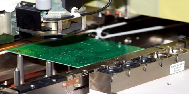
The PCB Fabrication process
PCB production shall be the process or process by which a circuit board design is transformed into a physical structure based on the requirements of the design kit. The following acts or methods accomplish this physical manifestation:
- The desired layout on laminates covered in copper.
- Excess copper from inner layers may be grated or removed to display traces and pads.
- Create the PCB layer stack at high temperatures by laminating (heating and pressing) board materials.
- Drill hole for holes, pins, and vias hole mounting
- Remove excess copper from the surface layers to disclose traces and pads.
- Boiler boxes and openings
- Adding surface or solder masking protective coating
- Silkscreen printing reference and markers of polarity, logo, or other surface markings
- Optionally, copper areas of the surface can be finished.
Is the PCB Fabrication process essential to understand?
The question is, “Is it necessary to understand the Fabrication process of PCB?” After all, PCB Fabrication is not a design company; it is an outsourced operation carried out by a contractor (CM). While Fabrication is not a design job, it is done in strict compliance with the requirements that you give your CM.
In most cases, the CM is not confidential to your design or efficiency goals. You will therefore not know if you make good choices in terms of materials, layout, locations or forms, trace parameters, or other board factors during Fabrication, and that can affect your production rates, production yield, or output after use, as described below:
Fabricability: Your steel fabricators capabilities rely on a variety of design choices. These include ensuring sufficient clearance between the surface elements and the board border and ensuring that the materials selected have a sufficiently high thermal expansion (CTE) coefficient to withstand PCBA, especially for non-lead soldering. Both could lead to the inability to construct your Board without a redesign. In addition, if you plan to panel your designs, you will also need to be careful.
Yield rate: Your Board can be produced successfully through Fabrication problems remain. For example, defining parameters that extend the tolerance limits of your CM device can lead to an unacceptable number of boards.
Reliability: It is graded according to IPC-6011 depending on the planned use of the Board. For rigid PCBs, three classification levels set specific criteria for a specific level of performance reliability that your Board must fulfill. Your Board would probably trigger inconsistent operations or premature board failure if designed to meet a lesser classification than your application needs.
The above examples are not exhaustive but reflect the types of problems you might have if the correct Fabrication specifications are not taken during design.
The response is, therefore, a strong yes! It is crucial to understand the PCB Fabrication process as the design choices you make in this stage will reverberate in the growth, production, and even PCB operation. Your best defense against the types of problems that cannot arise from your design choices is to use the rules and guidelines for design for manufacturing (DFMs) based on the capacities of your CM.
For DFM to be used to prevent better unnecessary delays and additional production costs, a complete and capable PCB design study, such as the one provided by Cadence, must be used. You can generate several comprehensive views with packages such as the Document Automation Tool to assist your CM in the Fabrication Process.
PCB is one of the most experienced customer service providers in China. Understanding that our customers’ success measures our performance, we concentrate on the attention and attention to details required for every PCB production phase. We also have vacuum packing, weighting, and shipping to ensure that your PCB order is secure and damage-free. We have so far printed platforms for companies of all sizes from more than 80 countries, and in the coming years, our goal is to supply our manufactured PCBs to every corner of the world.